Laser technology album
1. LASER SPOT WELDING
Type of connection — butt, lap. Thickness of welded edges — 0,05 mm - 2 mm. Diameter of welded wires — from 0,015 mm. Time of one spot welding up to 20 ms. On air and in inert gas jet
2. LASER SUTURAL WELDING

Sutural butt welding
Shunt (copper-manganin)
Length 13,4 mm, width 0,5 mm
Type of connection — butt, lap. Thickness of welded edges — up to 10 mm.
Welding velocity — 3 m/min (thickness 0.6 mm). On air and in inert gas jet.
Leak-proof welding of cases of solid-state devices in the monitored environment.
3. LASER DRILLING

BN covered with pyrographite
Diameter of holes 50 µm
Maximal thickness of drilled metal — 28 mm. Diameter of holes — 0,05-0,35 mm by copying method. Time of drilling — up to 5 s. Accuracy — ±10% from diameter.
Thickness 0,3 mm and less, diameterof holes 0,005-0,35 mm by copying method. Time of drilling — up to 1 s. Accuracy — ±5% from diameter.
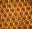
Calibrated holes from 3 µm in metal, thickness 20-100 µm; diameter from 50 µm in metal, thickness from 0,05-6 mm
4.LASER CUTTING

Width
0,02–1 mm
Materials: molybdenum (Mo), hafnium (Hf), nickel (Ni), rhenium (Re), tungsten (W), stainless steel, ceramics. Width 0,02-1 mm. Cutting velocity — up to 0,3 m/min. Cleanness of cut by RZ — up to 0,005 mm.
With high power gas lasers:
- Carbon steel. Width up to 28 mm. Cutting velocity 0,6-6 m/min.
- Stainless steel. Width up to 8 mm. Cutting velocity up to 1 m/min.
- Aluminum alloys. Width up to 10 mm. Cutting velocity up to 2 m/min.
- Copper Width up to 2 mm. Cutting velocity 0,3 m/min.
- Wood. Width up to 16 mm. Cutting velocity up to 6 m/min.
- PMMA. Width up to 80 mm. Cutting velocity up to 0,5 m/min.
Grids for electronic devices out of metals, graphyte, BN. Width 0,05-0,5 mm, width of crossbar from 0,02 mm, masks for deposition and sedimentation of coatings for frit deposition in thick-film technology.
5. LASER GRAVING AND MARKING

Laser deep graving, depth up to 0,5 mm; marking of metal and nonmetallic workpieces (deposition of trademarks, inscriptions etc.), manufacturing of labels
6. LASER PROCESSING OF THIN FILMS

Trimming of thin-
and thick-film
resistors
Laser trimming of different materials with high range of configuration/
Treatment of films: Ni, Cr, pyrographyte etc.
Glass and ceramics substrates; deposition of topology, restoration of photomasks; adjustment of absorbers.
7. LASER PYROLYSIS
Local coatings deposition on metals from gas ambience CnHn (methane, heptane). Deposition on grids directly on electrodes.
8. LASER DEPOSITION OF FILMS
Laser oxidation, deposition of osmium and thorium films.
9. LASER SOLDERING

Soldering of hinged elements of hybrid integral schemes
Soldering of internal lamp elements, coaxial connections, input-output knots.
Efficiency is 10-12 times more, than with electronic beam soldering.
10. LASER MICROSPECTRAL ANALYSIS (LIBS)

Emissin spectrum
Quantitative and qualitative emission spectral analysis of elemental composition of technical and biomedical objects: metals, alloys, dielectrics, electronic devices, glass.
Identification of depositions and coatings of different origin, width from 6 µm
Organic objects study (bones, hair, teeth etc.)
Limit of detection from 10-10 g; relative limit — from 0,001%.
Minimal spot size — 10 µm.
Pulse power density — 108-109 W/cm2.
Laser source — Nd:YAG (τ ~ 10 ns, q ~ 10-10-10-12 W/cm2).


